Smart tech driving company's growth


Applied Materials is a company that lives on the cutting edge.
Innovation and the ability to anticipate customers’ needs and then provide those products have pushed the Silicon Valley-based company to the No. 1 spot in the semiconductor and display equipment business. Revenue for the company’s fiscal year that ends Oct. 31 is expected to be $14.5 billion.
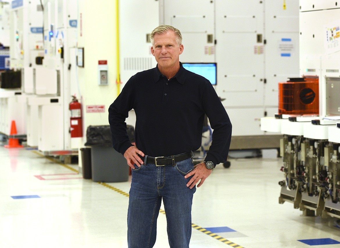
The Kalispell facilities are a pivotal part of the company’s success, said Rick Plavidal, general manager of Applied’s Kalispell business unit.
Applied Materials paid $364 million in 2009 to acquire Semitool, a company founded by Ray Thompson in the late 1970s that became a key player in the semiconductor industry.
Thompson championed Applied Materials for its global presence and ability to mass-market the Kalispell-based business. The acquisition was hailed by both companies as a collaborative move that would allow Applied to broaden its range of products and take advantage of a global recovery in the semiconductor industry.
And that’s exactly what has happened. Driven by an “explosion of data” needed for smart technology and the development of artificial intelligence-based technology, data has become the new oil, said Joe Pon, an Applied Materials corporate vice president.
By 2020 the entire state of Montana — roughly 1 million people — will generate 200 million gigabytes of data each day, and only 1 million of those gigabytes will be generated by humans, Pon said. Smart buildings will generate 55 million GB per day; smart factories will generate another 50 million GB; and smart vehicles will contribute 40 million GB daily.
“Processing the information, that’s the big part of AI (artificial intelligence) people aren’t necessarily seeing,” Pon said. “I think we’re just at the beginning … I can’t tell you how much pressure that puts on the semiconductor industry, to do diagnostics better, to make the rest of this future possible.
“There are some big waves coming forward with moving to artificial intelligence,” he continued. “There’s so much coming that will continue to put pressure to semiconductor industry. It’s changing physically the way we make the chips, so it can access larger amounts of data.”
Applied Materials operated Semitool for several years as a business unit of the Silicon Systems Group.
Four years ago the Semitool name went away and the Kalispell business unit — the main manufacturing and assembly plant on West Reserve Drive — was renamed the PPC (packaging, plating and cleans) Business Unit to better define that facility’s role, Plavidal explained. Applied also operates a machining and welding center with plastics expertise at an 80,000-square-foot facility at the northwest corner of U.S. 2 E. and Birch Grove Drive.
“We’ve done a good job of becoming part of the Applied family,” he said. “There’s been a theme of trying to integrate the Montana facilities.”
For those outside the semiconductor industry, what goes on inside the high-tech environment of Applied Materials can be difficult to comprehend. Simply put, the Kalispell PPC business unit designs, engineers and manufactures tools for some of the manufacturing steps that produce components used inside everyday tech products such as memory boards, processors and sensors for computers, smartphones and consumer electronics.
“We make the tools that make the chips and sensors,” Plavidal said.
Applied Materials employs 500 people between the two Kalispell facilities. A facility in Libby that employed about 40 has closed.
While there’s a logistical challenge of doing business in a rural place like the Flathead Valley, it hasn’t affected Applied Materials’ growth.
“Montana is a harder place to get people to move to,” Plavidal acknowledged, though he added once employees and their families experience living in the Flathead they tend to love it. “We also have more stable employment.”
The company takes advantage of engineering programs at Montana universities, often recruiting new engineers who have graduated. The type of hands-on work done at the Kalispell facilities is a drawing card for engineers.
Pon said Applied Materials has an extraordinary blend of innovators and “incredibly practical” engineers that drive the company forward.
“Our products in Montana are good examples of that,” Pon noted. “Today, pretty much every chip is made using our technology. We really think of ourselves as enabling the eyes and the brain for modern electronics.”
The company has capitalized on innovation and entrepreneurship since Day One. Michael McNeilly was only 28 years old when he signed the papers at his kitchen table on Nov. 10, 1967, that launched Applied Materials. He rented a small industrial unit in Santa Clara, California, and spent the next 10 years as CEO, growing his entrepreneurial endeavor from zero to $20 million.
“He was very smart and very savvy,” Pon said.
One of McNeilly’s best attributes was his ability to find out not only what was on his customers’ road map but also how he could help.
“They trust you to build the next thing that will help,” Pon said. “We still have that kind of attitude today. We transform possibilities into reality.”
The company has a global reach these days, operating in 82 locations in 17 countries.
Applied Materials invests 15 percent of its revenue directly back into research and development. The company has 10,200 patents and applies for an average of more than four patents every day of the week, Pon said.
“Because of that, 40 percent of our revenue comes from products introduced in the last few years … you’re only as good as the next problem you can solve.”
It’s no secret technology is becoming more complex.
A smartphone has 10 miles of wire in it, Plavidal pointed out.
“If you went back to 1960s technology, you’d virtually need a power plant to drive it,” he said.
Pon said a decade ago the company used a dozen materials from the periodic table of chemical elements. Today, Applied Materials uses about four dozen elements.
“It’s one atomic layer at a time, one thin layer of atoms and we have products that can find defects,” Pon said. “At 50 years old we’re setting new records for performance.”
Features editor Lynnette Hintze may be reached at 758-4421 or lhintze@dailyinterlake.com.